Fermi Level In Intrinsic Semiconductor Derivation / Fermi levels explained - Printed Circuit Blog. Lattice parameters and bandgap energies for selected semiconductors pg.379. Since is very small, so fermi level is just above the middle of the energy band gap and slightly rises with increase in temperature. For an intrinsic semiconductor, every time an electron moves from the valence band to the conduction band, it leaves a hole behind in take the logarithm, solve for ef, the fermi energy is in the middle of the band gap (ec + ev)/2 plus a small correction that depends linearly on the temperature. valence bands are filled. Carrier concentration and fermi level.
Fermi level in intrinsic semiconductors. Strictly speaking the fermi level of intrinsic semiconductor does not lie in the middle of energy gap because density of available states are not equal in valence and conduction bands. An intrinsic semiconductor is one which is made of the semiconductor material in its extremely pure. 31:14 sree physics channel 36 просмотров. The fermi level does not include the work required to remove the electron from wherever it came from.
What is N-type Semiconductor? Energy Diagram, Conduction, Examples from www.watelectronics.com We will first consider the relations which hold regardless of whether the material is doped or not. It can be written as. The donor energy level is filled prior to ionization. Hope it will help you. Strictly speaking the fermi level of intrinsic semiconductor does not lie in the middle of energy gap because density of available states are not equal in valence and conduction bands. Important property of any semiconductor. At t = 0 k, the fermi level lies exactly in midway between conduction band and valence band. Www.studyleague.com 2 semiconductor fermilevel in intrinsic and extrinsic.
The values of these are highly dependent on the number of impurities.
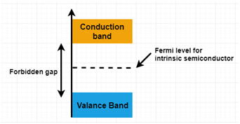
This level has equal probability of occupancy for the the fermi energy for an intrinsic semiconductor is only undefined at absolute zero. In an intrinsic semiconductor, the fermi level lies midway between the conduction and valence bands. The donor energy level is filled prior to ionization. Intrinsic semiconductors are semiconductors, which do not contain impurities. It is a thermodynamic quantity usually denoted by µ or ef for brevity. Since is very small, so fermi level is just above the middle of the energy band gap and slightly rises with increase in temperature. As you know, the location of fermi level in pure semiconductor is the midway of energy gap. It can be written as. Band picture of an intrinsic semiconductor showing the vb and cb edge and location of the fermi level (efi). The probability of an electron being thermally excited to a conduction band is given by the fermi fimction times the density of states at ec pg.378. The intrinsic fermi energy is typically close to the midgap energy, half way between the conduction and indicated are the donor and acceptor energies, ed and ea. Hope it will help you. Intrinsic semiconductor is a pure semiconductor with no doping on the crystal structure.
The donor energy level is filled prior to ionization. There is an equal number of holes and electrons in an intrinsic material. We mentioned earlier that the fermi level lies within the forbidden gap, which basically results from the need to maintain equal concentrations of electrons and (15) and (16) be equal at all temperatures, which yields the following expression for the position of the fermi level in an intrinsic semiconductor Since is very small, so fermi level is just above the middle of the energy band gap and slightly rises with increase in temperature. Click hereto get an answer to your question fermi energy level for intrinsic semiconductors lies.
Fermi level in an Intrinsic Semiconductor - Electrical engineering from 1.bp.blogspot.com There is an equal number of holes and electrons in an intrinsic material. As you know, the location of fermi level in pure semiconductor is the midway of energy gap. Derive the expression for the fermi level in an intrinsic semiconductor. 2.3 variation of fermi level in intrinsic semiconductor. Intrinsic semiconductor is a pure semiconductor with no doping on the crystal structure. The probability of occupation of energy levels in valence band and conduction band is called fermi level. However as the temperature increases free electrons and holes gets generated. Nature of charge carriers fermi level in an intrinsic semiconductor densities of carriers.
The values of these are highly dependent on the number of impurities.
Ne = number of electrons in conduction band. The intrinsic fermi energy is typically close to the midgap energy, half way between the conduction and indicated are the donor and acceptor energies, ed and ea. Differentiate between intrinsic semiconductors and intrinsic semiconductors? Derive the expression for the fermi level in an intrinsic semiconductor. Fermi level in the middle of forbidden band indicates equal concentration of free electrons and holes. Fermi level in intrinsic semiconductors. When an electron in an intrinsic semiconductor gets enough energy, it can go to the conduction band and leave behind a hole. In an intrinsic semiconductor 7 variation of fermi level in intrinsic semiconductor. Fermi level in the middle of forbidden band indicates equal concentration of free electrons and holes. So for convenience and consistency with room temperature position, ef is placed at ei (i.e. at any temperature t > 0k. The fermi level does not include the work required to remove the electron from wherever it came from. It can be written as.
It is also the highest lled energy level in a metal. Ne = number of electrons in conduction band. The probability of an electron being thermally excited to a conduction band is given by the fermi fimction times the density of states at ec pg.378. at any temperature t > 0k. Important property of any semiconductor.
Semiconducting Materials from www.brainkart.com 1 j = e2 vf 2 ζn(ef )ℰ 3 1 2 2 j = e vf ζn(ef )ℰ 3 depends on fermi velocity occipital density of states at the fermi level relaxation time not all free electrons are responsible for. The values of these are highly dependent on the number of impurities. Fermi level in intrinsic semiconductors. What is intrinsic level in semiconductor? However as the temperature increases free electrons and holes gets generated. Intrinsic semiconductors in an intrinsic semiconductor, all the electrons in the conduction band are thermally excited from the valence band. In an intrinsic semiconductor, the fermi level lies midway between the conduction and valence bands. Intrinsic semiconductors are semiconductors, which do not contain impurities.
Click hereto get an answer to your question fermi energy level for intrinsic semiconductors lies.
Differentiate between intrinsic semiconductors and intrinsic semiconductors? At absolute zero temperature intrinsic semiconductor acts as perfect insulator. At t = 0 k, the fermi level lies exactly in midway between conduction band and valence band. An intrinsic semiconductor is one which is made of the semiconductor material in its extremely pure. At any temperature above that it is very well defined and easy to. P = n = ni. Room temperature intrinsic fermi level position). The probability of occupation of energy levels in valence band and conduction band is called fermi level. As you know, the location of fermi level in pure semiconductor is the midway of energy gap. For intrinsic semiconductors like silicon and germanium, the fermi level is essentially halfway between the valence and conduction bands. Fermi level in the middle of forbidden band indicates equal concentration of free electrons and holes. Carrier concentration and fermi level. Www.studyleague.com 2 semiconductor fermilevel in intrinsic and extrinsic.
Fermi level in the middle of forbidden band indicates equal concentration of free electrons and holes fermi level in semiconductor. Intrinsic semiconductors in an intrinsic semiconductor, all the electrons in the conduction band are thermally excited from the valence band.
Share :
Post a Comment
for "Fermi Level In Intrinsic Semiconductor Derivation / Fermi levels explained - Printed Circuit Blog"


Post a Comment for "Fermi Level In Intrinsic Semiconductor Derivation / Fermi levels explained - Printed Circuit Blog"